 EN
EN

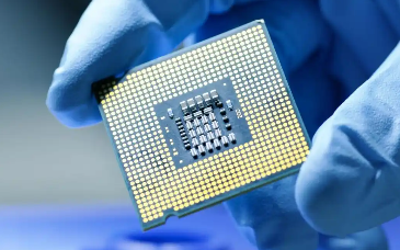
PCB Assembly Capability
| PCB Assembly Lead Times | From 24 hours to 7days once all parts are ready: |
| - Express turnaround: 24-hour assembly after component readiness | |
| - Standard production: Up to 7-day completion when sourcing from(all parts verified) | |
| Component Procurement Options | Full turnkey: Comprehensive component sourcing |
| Partial turnkey: Hybrid customer-supplied and FDPCB-sourced parts | |
| Kitted/Consigned: Complete customer-provided components | |
| Advanced Assembly Technologies | Surface Mount Assembly (SMT): High-precision chip placement |
| Ball-Grid-Array Assembly (BGA): 0.25mm pitch with mandatory X-ray validation | |
| Through-Hole Assembly (THT): Traditional component mounting | |
| Mixed technology: Combined SMT & Thru-hole solutions | |
| Mixed Assembly: Integrated SMT and Thru‑hole soldering process (reflow + wave/manual soldering) | |
| Kit Assembly: Component kitting according to BOM for streamlined manual or automated assembly | |
| Solder Types | Substrate Specialization: Rigid PCBs, Flex Circuits, Metal-Core Boards, Rigid-Flex PCB |
| Component Types | BGA: 0.25mm pitch with X-ray QA |
| Ultra-miniature: 01005/0402 passives | |
| High-density: Fine-pitch components as small as 0.38mm pitch ICs | |
| Connectors: Hard metric & cable assemblies | |
| Cable & Wire: Multiconductor cable and wire harness assemblies, enabling organized, insulated routing of multiple conductors within one outer jacket | |
| Bulk: Loose-packaged discrete components (resistors, capacitors, ICs, etc.) | |
| Assembly Side(s) | Single/Double Sided: Supports both single- and double‑sided board assembly |
| SMT Parts Presentation | Cut tape: Components supplied on cut tape, ideal for small quantities |
| Partial reel: Components on partial reels, suitable for mid‑volume usage | |
| Reel: Full‑reel packaging, the standard for high‑volume SMT components | |
| Tube: Components packaged in tubes, typically for cylindrical or long parts | |
| Tray: Supplied in trays, used for large or sensitive components | |
| Laser-cut stainless steel: Delivered on precision laser‑cut stainless steel carriers for high‑precision or specialty components | |
| Quality Inspection & Testing Protocols | Visual inspection: Manual visual inspection of the PCB using magnifying tools to identify component placement, solder joint quality, and other visible defects. |
| AOI Scanning: Utilizes automated equipment to scan the PCB, detecting component absence, solder joint issues, polarity errors, and more. | |
| BGA placement – X-RAY checking: Employs X-ray technology to inspect internal solder joint quality of BGA, QFN, and other packages, ensuring no cold solder joints or bridging. | |
| In-Circuit Test (ICT): Conducts electrical tests to verify connectivity and functionality of circuits on the PCB, detecting issues like shorts and opens. | |
| Functional Testing(FCT): Tests the PCB's functionality under actual operating conditions to ensure it meets design specifications and performance requirements. | |
| After-Sales Service Commitment | Should your assembled PCBs encounter transit issues or potential defects upon delivery, we provide immediate repair and rework assistance. Our dedicated engineering team stands ready to resolve concerns through prioritized communication ensuring swift solutions that maintain project momentum and uphold our quality partnership. |
Disclaimer:The materials on this website are collected and sorted from the Internet. The copyright of the works belongs to the author. If it infringes your copyright, please send an email to us


_复制.png)