 EN
EN

Experience sharing of multilayer PCB impedance wire routing
In daily life, we come into contact with mobile phones, computers, and high-definition TVs every day, and their core is the circuit board, which is inseparable from impedance matching in order to achieve high-speed data transmission.
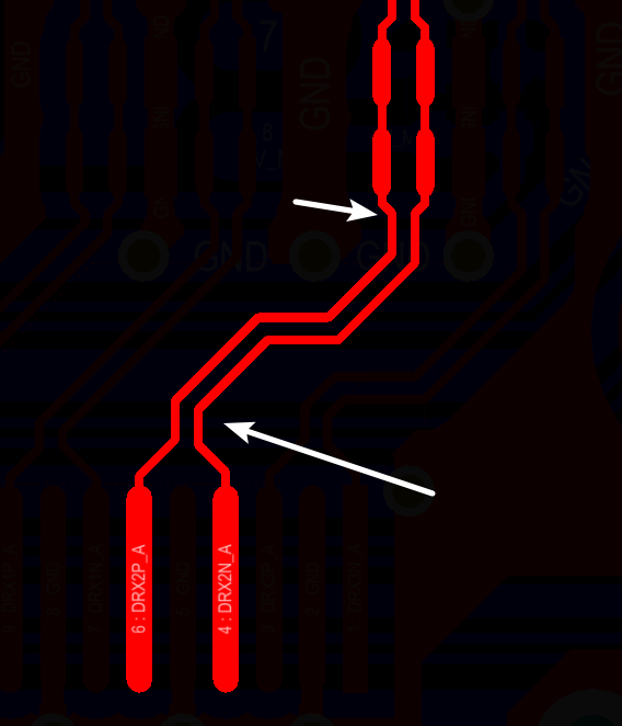
For example, the mobile phone USB interface, it can transmit data synchronously in both directions, fast speed, low cost, the two most common types are Type-A, Type-B, Type-C. In the definition of USB protocol, (D+, D-), (TX+, TX-), (RX+, RX-) differential signal lines transmit digital signals, in order to ensure the stability of the transmission signal, effectively cancel the common mode interference of the external boundary, and suppress EMI, the circuit board design differential wire must be arranged in strict accordance with the wiring rules of the differential signal.
Huaqiu circuit summarizes the following points: 1. The devices should be as close as possible during the layout, shorten the distance between the devices to make the difference line the shortest, and try to punch as few holes.
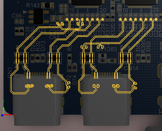
2. The wire routing should be parallel and symmetrical, and the corner line should not be taken according to 90°, and the line spacing should be controlled within 2W as much as possible.
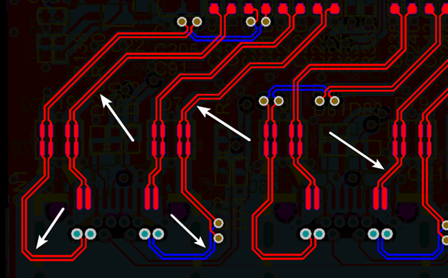
3. When connecting resistor capacitors in series, the resistor capacitors are aligned up and down or left and right.
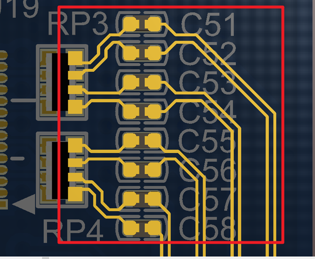
4. The differential line should be equal and equidistant as much as possible to avoid timing deviation and common mode interference.
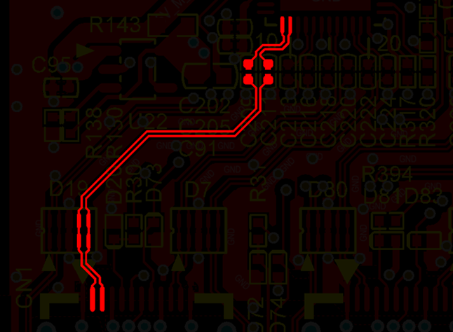
5. Due to factors such as pin distribution, vias, and trace space, the differential line length is easy to mismatch, and once the line length is not matched, the timing will be shifted, and common-mode interference will be introduced, reducing the signal quality. Therefore, it is necessary to compensate for the mismatch of the difference pair, so that the line length matches, and the length difference is usually controlled within 5mil.
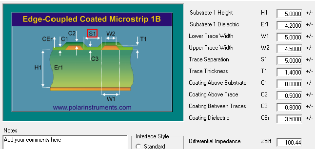
The impedance calculator used in the factory is Polar Si9000, the parameters are as follows:
H1: Dielectric thickness (thickness between the impedance line and the reference layer)
Er1: Dielectric constant of the plate 4.2-4.6 (PP is calculated as 4.2, Coer is calculated as 4.5)
W1: Design line width W2: Top line width = Design line width minus 0.5mil
S1: Distance between two lines T1: Copper thickness,
C1: Green oil thickness on substrate surface
C2: Green oil thickness on copper foil surface
C3: Green oil thickness on substrate surface
CEr: Dielectric constant of green oil 3.5


_复制.png)